")
")

The LIGA-process is used to manufacture micro structures by deep X-ray lithography. LIGA is the german acronym for lithography, electroplating and moulding (Lithographie, Galvanik und Abformung). The LIGA-process has been developed in the "Institut für Kernverfahrenstechnik" (IKVT), today "Institute for Microstructure Technology" (IMT) in the Forschungszentrum Karlsruhe GmbH since the late 1980th [Sai 2008]. Today several institutes use the LIGA-process, e.g. [Goe 2006].
Primarily the LIGA-process provides high aspect ratio micro structures in polymers like e.g. PMMA (better known as acrylic glass). Via electroplating these structures can be replicated in metals like gold, nickel, magnetic nickel-iron alloys or copper. Even replications in ceramics are possible. An industrial low cost production of micro structures is possible when a nickel tool is fabricated for hot embossing or injection moulding.
The main characteristics of LIGA-structures are:
- large layout freedom in the mask geometry
- high aspect ratios of up to >100 achievable
- parallel side walls with flank angle very close to 90° (deviation: about 1 µm for 1 mm high structures)
- smooth side walls (Ra in the 10 nm range) suitable e.g. for optical micro mirrors
- lateral precision in the few micrometre range over distances of several centimetres
- structural details on side walls in the 30 nm range possible
- different side wall angles via double exposure possible
The LIGA-process includes these principal steps:
| 1. | Making an intermediate X-ray absorption mask (IM) with about 2.2 µm high gold absorber structures by electron beam writing. | |
| 2. | Copying the intermediate mask into a working mask (WM) with about 25 µm high gold absorber structures by X-ray lithography. | |
| 3. | Copying the working mask to 100 µm to 3000 µm high micro structures by deep X-ray lithography. | |
| 4. | a) | Electroplating metals like gold, copper or nickel into these structures to form metal micro structures. |
| b) | Making a several millimetre thick mould from these structures by nickel electroplating. | |
| 5. | Mass replication of the mould into thermoplastic resin. |
The process steps are illustrated in the figures (all: ©01) below. All steps in this illustration are carried out with positive resists, i.e. resists that can be dissolved after electron beam or X-ray exposure. The process steps are described in detail below the figures.


")
")


The LIGA-process (as it is used in the IMT) in detail:
1. Fabrication of an intermediate mask (IM):
First an intermediate X-ray absorption mask (IM) is made by electron beam writing a CAD generated layout into a resist layer (fig. 5). As substrate normally a silicon wafer is used, just because it is flat, smooth and not to expensive (fig. 1). This substrate is coated with a carbon layer in a sputter process. This layer is needed later to be able to separate the mask from the substrate. At the border of the wafer a few millimetres remain uncoated (fig. 2). Then the whole wafer is coated with a 2 µm thick titanium layer in another sputter process (fig. 3). The titanium will not stick to the carbon layer, but to the silicon wafer where the silicon is visible. This prevents the titanium layer to lift of from the wafer by internal stress. Titanium (low atomic number!) is used, because of its good transparency for X-rays. After this the wafer is spin coated with a 3.5 µm thick PMMA resist layer (fig. 4). PMMA is a positive resist. In the electron beam exposure step, in resist areas hit by the electrons, the long PMMA-molecules are damaged and can be dissolved in the following development step (fig. 6). In some cases also negative resists are used. These are cross-linked by the exposure, so exposed areas remain after the development process. Subsequently a 2.2 µm thick gold layer is deposited on the titanium layer where no resist covers the titanium (fig. 7). Gold (high atomic number!) is used because of its high X-ray absorption coefficient. In this step the thickness of the gold is critical: when the gold is overgrowing the resist layer, the wanted geometry of the mask is lost and it becomes useless. In the next step the remaining resist is dissolved in a solvent suitable for non-exposed PMMA (fig. 8). Then a 6 mm thick invar-steel (mechanically invariant to temperature changes) frame is glued onto the titanium membrane, giving mechanical stability to the fragile membrane (fig. 9). With a knife the titanium membrane is cut through at the outer contour of the frame (fig. 10) and the mask (fig. 12) is carefully separated from the substrate (fig. 11). The X-ray absorption contrast of the intermediate mask is sufficient to produce structures of up to about 70 µm thickness by X-ray lithography. As in most cases this height will not be sufficient, a so called working mask with a higher X-ray absorption contrast is needed.
2. Making a working mask (WM):
A working mask is an X-ray lithographic copy of an intermediate mask with the aim to get a mask with a higher X-ray absorption contrast. One way to make a working mask starts with a steel plate with a polished front side (fig. 13). The back side of this plate is thinned by milling, leaving only a wall of a few millimetres (fig. 14). The front side is coated with a 2 µm titanium membrane by sputtering (fig. 15). Then a 60 µm thick PMMA resist layer is deposited on the titanium membrane (fig. 16). The resist layer is structured by X-ray lithography via the intermediate mask (fig. 17). After developing the exposed areas (fig. 18) 25 µm thick gold absorbers are electroplated (fig. 19). Subsequently the remaining resist is exposed to X-rays without using a mask, so it can be stripped afterwards in the same developer (fig. 20). The last step is to etch the cavity in the back side of the mask with a selective etching medium, so the steel is removed and only the free standing titanium membrane is remaining (fig. 21).
3. Producing high aspect ratio resist structures by deep X-ray lithography:
In the deep X-ray lithography step a shadow projection of the working mask into a quite thick PMMA resist layer (100 µm to 3 mm) is performed (fig. 22, 23). PMMA layers of this thickness mostly are glued to the substrate. Normally a proximity distance of 50 µm to 150 µm is introduced between the mask and the resist surface to protect the mask from damages that might result from a contact between mask and resist. The direct lithographic micro structure is finished after a development step (fig. 24).
4. Electro forming:
When metal micro structures are required, an electro forming step is added. In this case the micro structures are fabricated on an electrically conducting substrate or the substrate and the micro structures are covered with a thin layer of e.g. gold. Then, in the electro forming step the required metal is deposited (fig. 25). When the process is stopped before the metal layer is higher than the resist structure, the produced structures can be used as metallic micro structures. As the original resist micro structures still remain on the substrate, a flood exposure step (without mask) is introduced to be able to dissolve the resist structures afterwards (fig. 26). The metallic micro structures have to be separated from the substrate (fig. 27). This can be done by mechanical force when the surface of the substrate is very smooth, so the adhesion between the structures and the substrate is low. If the forces become to high, the micro structures might be deformed. In this case a sacrificial layer (e.g. titanium) on the substrate can be used. This layer is etched selectively (e.g. with HF), so the metallic micro structures are separated from the substrate (fig. 28).
When a mass production is required, a nickel mould has to be fabricated. In this case the electro forming step is continued until the deposited nickel layer has reached several millimetres in thickness (fig. 29, 30). Then this nickel block (fig. 31) is removed from the substrate (e.g. an 8 mm thick copper block) and by wire-cut electrical discharge machining it is brought into a precisely defined outer shape (fig. 32, 33). Again a flood exposure (fig. 34) is used to prepare the removing of the remaining resist in the mould (fig. 35).
5. Mass replication by hot embossing or injection moulding:
The nickel moulding tool can then be used several ten thousands of cycles to replicate micro structures via hot embossing or injection moulding (fig. 36). In the case of hot embossing the resulting structures mostly have to be machine finished (fig. 37).
The LIGA process in photos:
In the following, photos of the individual steps of the LIGA process give an impression of the laboratory reality and of typical occurring errors.
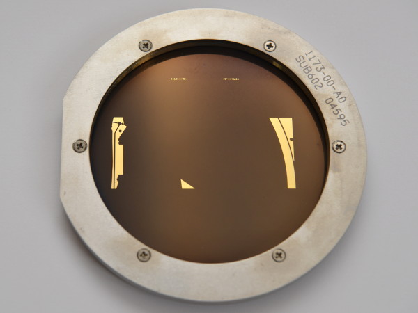
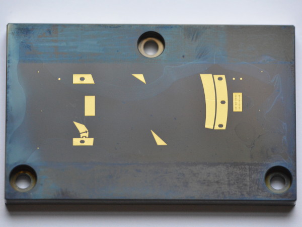
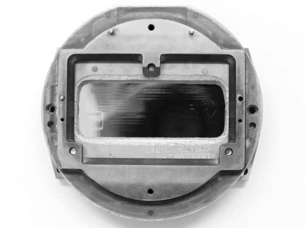
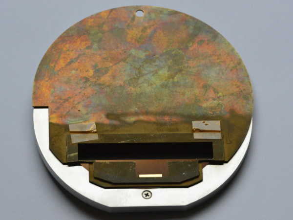
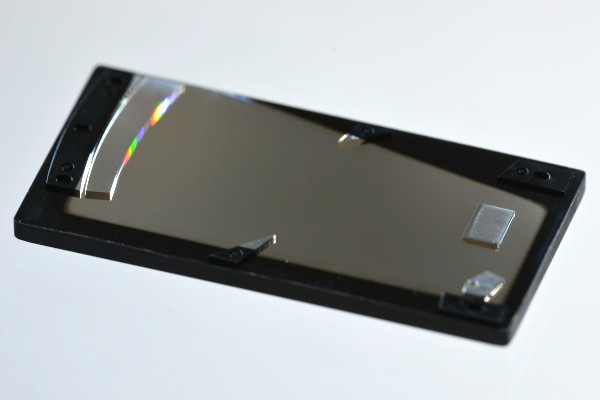
X-ray depth lithographic working mask for a microspectrometer, layout field 75 mm round, gold absorber on titanium membrane with invar frame (as Fig. 12). The working mask is made on a lift-off wafer, therefore the gold absorbers are on the frame side (©01).
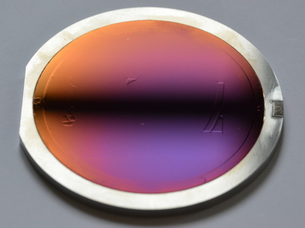
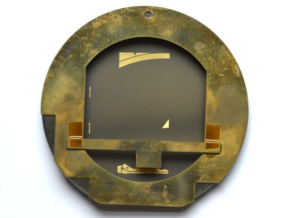
Rear side of the working mask (to Fig. 21): The gold absorbers on the rear side, which are caused by tension between the gold and the titanium membrane, can be seen through the titanium membrane. The colorful coloration comes from the intermediate layers between titanium and the lift-off absorber (©01).
Detail of the gold absorbers (with curved diffraction grating of a microspectrometer) on the titanium membrane; the colourful back of the membrane bulges upwards in the locations with gold absorbers. The stress peaks at the structural corners can lead to the rupture of the membrane (©01). 
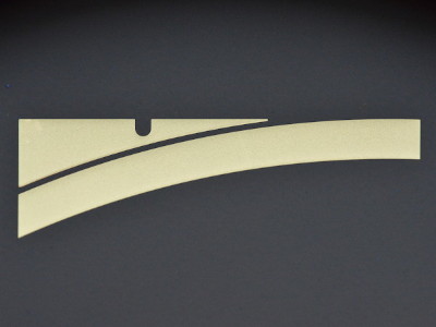
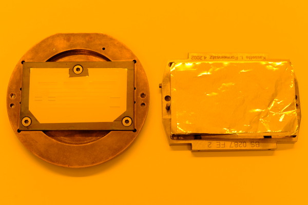
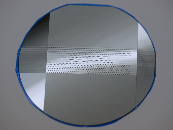
Deep X-ray lithography working mask for a microspectrometer with 20 mm x 60 mm layout field, gold absorber on titanium membrane with invar frame (to Fig. 20). The working mask is made on an invar substrate and etched free from the back side, therefore the gold absorbers are on the side facing away from the frame (©01).
Mask errors
Various mask errors can occur, of which some typical ones can be seen here.

The titanium membrane may rupture when lifting off from the lift-off substrate or spontaneously due to internal tension (©01).

When copying from the intermediate mask (left: with about 2.5 µm gold height on a 2.5 µm thick titanium membrane) over the working mask (with 25 µm gold absorbers) not shown here into a 340 µm high resist (right: PMMA), the structure fidelity (here teeth of a diffraction grating) decreases due to diffraction at the edges of the absorber structures and due to secondary electrons and X-ray scattering in the resist. The right picture shows the adhesive layer (dark grey) with which the PMMA platelet was bonded to the substrate (©01).


Sharp corners like the triangles in the left picture lead to cracks in the resist, into which gold might then be electroplated. Mostly, one tries to avoid curvature radii below 5 µm already in the layout, which is not always possible. The right image shows an overplated area. Here the gold has locally grown too fast and has exceeded the height of the resist. The intermediate mask has a defect at this point, because the overgalvanized gold leads to deviations from the desired shape in the working mask in the next step of the X-ray lithographic copy. As a preventive measure, the electroplating bath is filtered so that there are no gold particles in the solution that could settle on the substrate (©01).
Exposure
For deep X-ray lithographic exposure, the X-ray absorber mask and the resist to be exposed must be moved up and down in a scanner in vertical direction through the X-ray beam (at a bending magnet at a synchrotron radiation source in the form of a horizontal line a few millimeters in height) so that the entire layout area is exposed. For illustration purposes, the holders used at KIT are shown:

Holding plate 1 for the substrate with the photoresist, here a rectangular silicon substrate with 2 mm SU-8 resist. The resist looks liquid, but is hard. The substrate is glued to the holding plate with three adhesive strips. In a previous step (see Fig. 23), the microprisms of X-ray prism lenses have already been exposed perpendicular to the substrate, but the resist has not yet been developed, because in a further exposure step before development, support planes under ±45° are to be exposed. The mouse-over image shows three spacer blocks for adjusting the proximity distance between the working mask and the resist surface, and a Kapton foil (=polyimide) which, together with an aluminum foil (see next image on the right), absorbs the scattered long-wavelength radiation produced in the working mask. At the same time, the foil protects the working mask from coming into contact with the resist, which is slightly sticky and may foam up bubbly during irradiation. The image is orange because it is taken in the yellow light area. The yellow illumination prevents exposure of the resist by visible light (©01).
A second holding plate 2 (left) holds the mask, which is fixed with three screws. The resist holding plate (right) is covered with an aluminium foil as X-ray stray light filter. The two holding plates 1 and 2 are positioned to each other by means of two adjustment pins (visible on the side of the aluminium foil) and then installed as a block in the irradiation facility (©01).

Skin formation on the top side of the resist due to scattered X-ray light from the working mask. Skin formation can be avoided by using filter foils between the mask and the resist (©01).
Block from the two holders 1 and 2 seen from the mask side (©01).

Holder 3, which holds the block of holder 1 with resist and holder 2 with the mask. In the mouse-over picture from the back side (©01).

Holder 4, which is clamped together with holder 3, is inserted into the X-ray scanner for irradiation. This holder accommodates a cooling plate in the round recess to cool the irradiated sample heated by the X-rays. In the mouse-over picture from the back side (©01).

Block from holders 3 and 4, seen from the beam side. Here without mask and resist (©01).
Inclined exposures
To obtain structures that are inclined to the substrate surface, the working mask and resist can be tilted together against the direction of the incident X-ray radiation of the synchrotron source. If all structures should not have the same inclination, additional brass apertures can be used to protect parts of the layout from individual irradiation steps and only expose them at a different inclination angle in later exposure steps.
A 1 mm thick brass stop protects a partial area of the resist from the perpendicular exposure (©01).
In the next step the first brass stop is replaced by a second brass stop. The block of holders 1 and 2 is retained and with it the position of the mask to the resist. The block is tilted as a whole towards the incident X-ray beam and the previously protected area is then irradiated at an angle (©01).
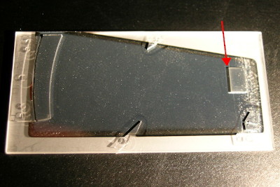
Molded polymer (PMMA) microspectrometer with 40° decoupling mirror (red arrow), which was structured by inclined exposure. The spectrometer is vapour deposited with aluminium in the area of the optical hollow waveguide. The coupling-out mirror reflects the spectrally split light coming from the self-focusing diffraction grating (left) onto a photodiode array. The 40° angle prevents light from the diode array from being reflected back into the hollow waveguide. For details see my dissertation Misguided light in LIGA microspectrometers (©01).
Structural defects
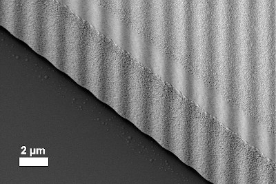
The LIGA process is used to produce microstructures with a high aspect ratio. The aspect ratio is defined somewhat imprecisely as the ratio of structure height to structure diameter. Of course, fine structures, like the teeth of the diffraction gratings shown above, which are structured adjacent to a wall, are mechanically much more stable than free-standing slender columns. Aspect ratios up to 120 are possible under favourable conditions. Free-standing columns with high aspect ratios are easier to fabricate than fields of columns standing close together.

125 µm high prisms with 15 µm edge length with triangular cross section (see X-ray prism lens), which are partially leaned against each other by capillary forces during drying after development (©01).
Separation of structures
To separate the microstructures produced by direct lithography, the silicon wafer can be cut up with a wafer saw or even lasered. The photo shows seven pairs of refractive X-ray lenses, which were separated for subsequent assembly (©01).
Fabrication of metallic microstructures
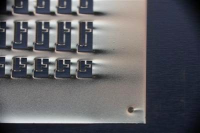
Electroplated microstructures show typical variations in height. The electrolyte has flowed over the sample from left to right in the picture. In the flow direction behind the PMMA microstructures, the gold thickness is higher than in areas between the microstructure rows. The turbulent flow behind the microstructures leads to an increased ion exchange at the metal surface, while in the horizontal trenches between the microstructures the laminar flow leads to a lower ion exchange and thus to lower growth rates. The best results are achieved when the whole layout area is evenly covered with structures. At the edge of the plating area (in the bottom of the picture) the so-called "bathtub effect" leads to higher structures, because here the electric field line density increases due to edge effects caused by the limited electrode area. In the mouse-over picture as video (17 MB, takes some time) (©01).
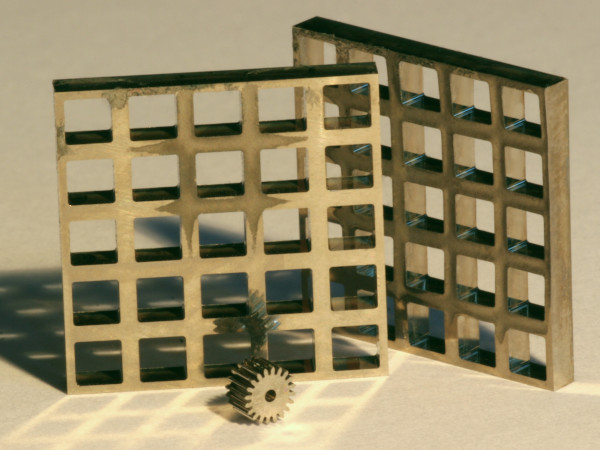
Electroplated microstructures and a gear wheel in about 2 mm high nickel; normally such structures are then polished on the top of the electroplated surface to achieve a constant structure height and shiny surfaces. The structures in the picture are not fully polished (©01).
Moulding tools
For the production of a nickel moulding tool with which inexpensive moulded plastic microstructures can be produced, an approximately 6 mm thick nickel layer is electroplated on a copper substrate onto which PMMA microstructures have previously been exposed. The microstructures are completely overgrown.
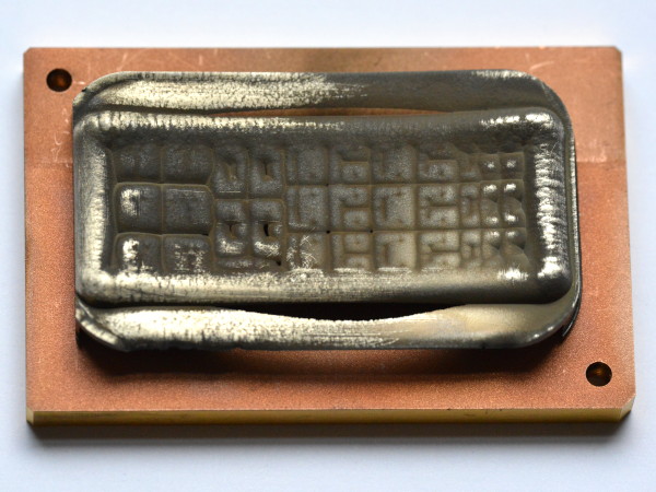
A rough image of the microstructures can still be seen on the nickel surface. This photo shows only the residual structures that remain after eroding the mould insert (see Fig. 31) (©01).
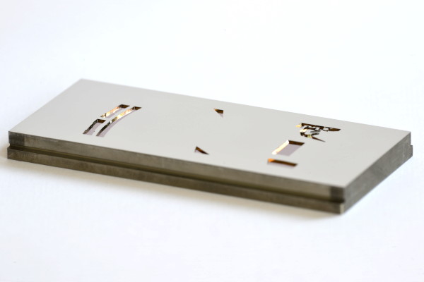
Finished mould insert for moulding a microspectrometer (see Fig. 35) (©01).
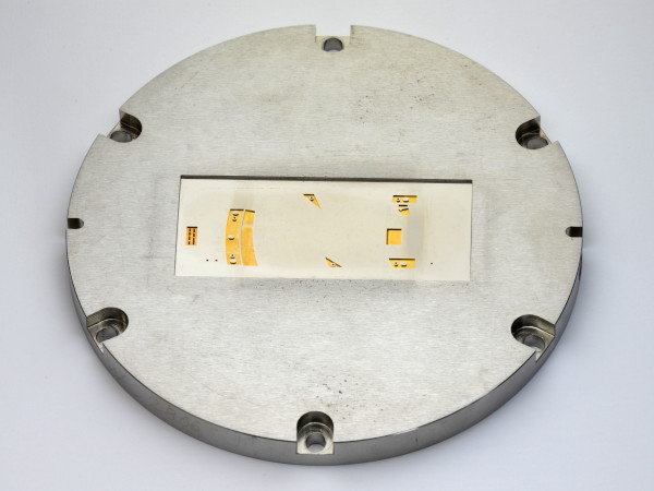
Mould insert inserted in the mould plate (©01).

Moulded PMMA spectrometer, still uncut (to see Fig. 36); in the mouse-over image coated with gold by evaporation (©01).
Moulded polycarbonate spectrometer coated with aluminium by vaporization, trimmed with focusing diffraction grating (spectrum on the left in the picture). In the mouse-over image spectrmeter in PMMA, where two structures have a greater height: for this purpose two cavities were electro-eroded into the mold insert (to Fig. 37). (©01).
| [Goe 2006] | J. Goettert, P. Datta, Y. Desta, Y. Jin, Z. Ling, V. Singh, LiGA Research and Service at CAMD, International MEMS Conference 2006, Journal of Physics: Conference Series 34, pp. 912–918, DOI: 10.1088/1742-6596/34/1/151, 2006 |
| [Sai 2008] | Edited by V. Saile, U. Wallrabe, O. Tabata, J. G. Korvink, LIGA and its Applications, Advanced Micro & Nanosystems, vol. 7, Wiley-VCH, ISBN 978-3-527-31698-4, 2008 |